
Atomera Inc’s MST Technology: Progress and Profitability Challenges in Semiconductor Licensing
Atomera advances its MST technology commercialization while grappling with persistent operating losses and complex industry adoption hurdles.
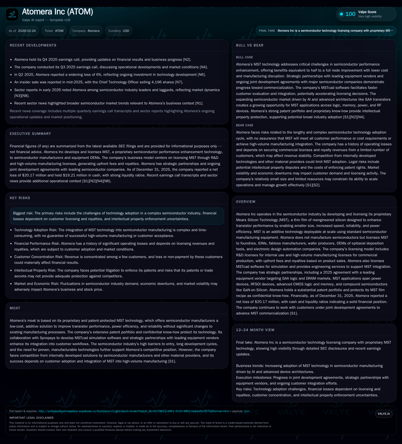
Atomera Inc specializes in licensing its proprietary Mears Silicon Technology (MST), a patented thin silicon film designed to enhance semiconductor transistor performance through an additive manufacturing-compatible process. Despite the technological promise and strategic collaborations spanning foundries, IDMs, and equipment OEMs, Atomera has generated minimal revenues and continues to incur sizable operating losses and cash flow deficits as it navigates extended integration and qualification phases inherent to semiconductor tech adoption. Key challenges include customer qualification delays, royalty realization uncertainties, intellectual property enforcement risks, and the longer time horizons typical for semiconductor materials licensing. Monitoring milestone achievements within joint development agreements and expansions of royalty-bearing licenses will be critical indicators of Atomera’s potential transition toward sustainable profitability.
Evolution of Atomic Innovation: Historical Performance and Revenue Trends
Atomera's journey since inception has been defined by protracted development of its MST technology—a patented reengineered silicon thin-film aimed at improving transistor size, speed, power efficiency, and reliability without requiring disruptive changes to existing CMOS fab processes [S17]. The company's revenue history underscores the early-stage nature of this business model. Annual revenues reached a modest $533K in 2019 before collapsing to only $62K in 2020 amid intensifying product development activities rather than commercial sales [F1].
Operating income has consistently reflected steep losses expanding from approximately -$17.5 million in 2022 to -$21.1 million in 2025, paralleled by net losses increasing to -$20.2 million in 2025 [F1]. Operating cash flow remains negative in excess of $14 million annually as Atomera sustains resource-intensive research, wafer processing on leased epi reactors, engineering services for customer integration, and software enhancements for MSTcad TCAD simulation tools.
This financial pattern typifies semiconductor material IP licensors transitioning through extended joint development agreements (JDAs) with key industry players as their technologies ascend from validation through product integration into high-volume manufacture.
Historical performance (annual)
| FY | Net ($mm) | CFO ($mm) | OpInc ($mm) | Capex ($) | Net YoY |
|---|---|---|---|---|---|
| 2025 | -20 | -15 | -21 | 49000 | -9.4% |
| 2024 | -18 | -13 | -19 | 14000 | +6.8% |
| 2023 | -20 | -15 | -21 | 31000 | -13.5% |
| 2022 | -17 | -12 | -18 | 39000 |
Note: Omitted columns lack sufficient annual XBRL coverage in the provided tags (need ≥2 annual points): Rev, Div, Buybacks. Source: SEC companyfacts cache [F1].
Capital returns and efficiency (annual)
| FY | FCF ($mm) | ROE% |
|---|---|---|
| 2025 | -15 | -109.8 |
| 2024 | -13 | -73.5 |
| 2023 | -15 | -108.9 |
| 2022 | -13 | -85.9 |
Source: SEC companyfacts cache [F1]. -6.4% |-6.8% |-9.1% | | 2025 | N/A |-21,123 |-20,174 |-14,871 |49 | N/A |-9.2% |-9.4% |-12.4% |
Note: Revenue figures post-2020 insufficient for YoY calculations; Operating income & net income available only from FY2022 onwards.
Overall trends illustrate a continued investment commitment despite limited near-term revenue realizations as Atomera aims to advance MST from technological promise toward licensing maturity.
Licensing Model and Customer Engagement in Semiconductor Ecosystem
Atomera operates under a nuanced technology licensing framework tailored specifically to the semiconductor value chain's complexities [S15][S22]. The company does not fabricate semiconductors directly but licenses its MST technology—including proprietary process recipes for depositing the MST thin film—to foundries, integrated device manufacturers (IDMs), fabless designers, wafer providers, epitaxial deposition tool OEMs ("epi tools"), and EDA software vendors.
Customers initially engage via paid evaluation arrangements or Joint Development Agreements (JDAs), which encapsulate stages combining engineering services such as wafer processing on leased epitaxial reactors (two leased reactors supporting both 200mm/300mm wafers facilitate internal R&D and customer trials), TCAD simulation using Atomera's MSTcad software integrated with Synopsys' Sentaurus platform for rapid modeling insights into expected device benefits [S11][S22], process integration testing on actual wafers shipped back-and-forth between Atomera and customers [S23], culminating in a phased license grant structure:
- R&D License: Grants internal-use rights for manufacturing MST-enabled wafers primarily for development/testing within the customer's fabs without external distribution rights.
- High-Volume Manufacturing (HVM) License: Enabled after successful qualification phases allowing customers to sell MST-enabled products commercially while paying upfront license fees plus ongoing royalties based on sales or wafer volumes.
For instance, Atomera maintains two active JDAs—one with a leading semiconductor provider that reached Phase Four installation enabling internal fab usage under paid manufacturing license but not commercial distribution—and another JDA with a major foundry wherein wafers are being actively run to demonstrate MST advantages towards qualifying HVM licenses [S5]. Additionally, integration license agreements exist with a leading fabless RF provider, an IDM/foundry partner Asahi Kasei Microdevices (AKM), and other entities currently engaged in Phase Three integration steps [S14].
The MSTcad simulation tools significantly shorten adoption cycles by guiding engineers where MST can deliver maximal benefit on analog, logic or memory products considering complex device physics nuances—an important aid given advanced node device fabrication complexity and escalating wafer costs that challenge direct physical trial-and-error approaches [S25][S11].
Roadblocks and Catalysts for MST Commercial Scaling
Despite technical progressions underscored by successful JDA milestones and equipment vendor partnerships enhancing epi tool integration processes [S15], commercial scaling of MST meets multiple headwinds:
- Customer Qualification Delays: Integration complexity during Phase Three testing leads to extended wafer runs requiring significant fab capacity allocation—often deprioritized against production demands—and iterative cycle times that lengthen decision timelines [S21].
- License Advancement Risks: The company’s efforts to convert R&D licensees into royalty-bearing HVM licensees remain nascent; delays or stalling at qualification phases increase revenue recognition latency risks [S1][S24].
- Intellectual Property Enforcement Uncertainty: While Atomera’s patent portfolio is extensive targeting foundational material innovations—the risk posed by potential patent challenges or infringement disputes poses operational backdrop uncertainty affecting negotiations [S4][S18]. Litigation costs could be substantial despite no current proceedings reported but ongoing enforcement vigilance is necessary.
- Competitive Landscape: Major semiconductor companies often develop internal materials/process enhancements competing directly with licensed technologies like MST; furthermore third-party alternatives from OEMs or universities also exist though Atomera claims superior patented efficacy [S18].
- Concentration Risks: Revenues rely heavily on few potential customers due to industry consolidation—loss or delayed progression of any major lead customer can materially impact future royalties given dependency on scale product shipments [S10].
Nonetheless catalysts exist including growing demand driven by AI applications pushing GAA logic architectures and DRAM markets that benefit directly from power-performance gains attainable via MST films incorporated using industry-standard epi tools leveraged in equipment vendor collaborations secured recently [N1][S11][S15].
Future Milestones and Industry Collaborations to Monitor
Explicit forward-looking guidance is absent due to intrinsic uncertainties in JDAs maturity timings yet several milestones serve as barometers:
- Successful achievement of Phase Four milestones within JDAs leading to execution of distribution agreements coupled with royalty-based commercial licenses represent key tipping points.
- Expansion from initial non-commercial paid manufacturing licenses toward full HVM licenses alongside royalty commencement signals transition from development spending to revenue generation phases.
- Conversion rates from MSTcad evaluators/licensees into full production licensees provide a readout on market acceptance velocity powered by simulation-led design cycle acceleration.
- Ongoing collaboration refinement under the partnership with major epi tool OEMs strategized around next-generation GAA logic transistors qualified through joint solutions enhances seamless MST adoption prospects.
Market observers should track announcements concerning wafer shipment commencements embedding MST at scale along with aggregate royalty receipts signposting commercial validation beyond R&D engagements [N1][S24][S11].
Capital Deployment, Liquidity State, and Return Metrics Analysis
Atomera maintains a strong liquidity position—with cash & cash equivalents reported at approximately $19.2 million at end-2025 against current liabilities near $2.0 million delivering an exceptionally healthy current ratio around 9.8x which provides operational runway prerequisites despite ongoing losses [F1].
Capital expenditures remain minimal reflecting the company’s IP licensor role rather than capital-intensive manufacturing profile: FY2025 Capex was just $49K compared with $14K-$39K range historically indicating focused spend largely related to epi reactor leases/maintenance or minor tooling upgrades rather than asset buildout.
However operating cash flows are consistently negative exceeding $14 million annually representing sustained burn amid R&D investments supporting wafer runs for customer validations and software platform upkeep—yielding an approximate free cash flow deficit near -$15 million excluding financing activities in recent years [F1].
The absence of dividend payments or share repurchases accords with typical early-stage IP licensing enterprises focusing resources on commercialization efforts rather than shareholder returns at this stage [F1][S26].
Utilizing trailing twelve-month net loss relative to equity produces an estimated ROE near -110%, highlighting continued unprofitability but consistent reinvestment aligned with long commercialization gestation periods intrinsic in semiconductor material innovation adoptions.
Intellectual Property Risks and Competitive Environment
Atomera’s moat rests squarely on its proprietary patent estate protecting the novel silicon thin-film innovation embodied in MST technology complemented by trade secret protections safeguarding know-how critical for manufacturability across standard epi deposition tool platforms used throughout semiconductor fabs globally [S17][S18].
Nevertheless litigation risks related to asserting these patents against infringing parties introduce substantial uncertainties both financially—due to unpredictable legal costs—and strategically if key patents were invalidated or narrowed damaging exclusivity claims consequently impacting licensing attractiveness [S4][S6][S18]. Such disputes could also influence negotiations indirectly if current or prospective licensees delay decisions awaiting outcomes.
Industry competition arises chiefly through:
- Internally-developed transistor enhancement approaches employed by leading IDM/foundry/fabless companies striving for differentiation without third-party dependence;
- Other external materials suppliers or research institutions presenting alternative solutions potentially overlapping some performance features of MST;
- Continuous innovation pressure driven by escalating node complexities requiring robust techno-economic justification for license uptake given capital intensity involved; which collectively impose nontrivial barriers even as Atomera leverages its mature TCAD software collaboration enabling targeted application identification shortening traditional trial periods.
Conclusion: Prospects for Transitioning MST from R&D to Sustainable Growth
Atomera sits at an inflection point typifying deep-tech licensor companies embedded within the semiconductor ecosystem characterized by prolonged product validation cycles preceding revenue realization milestones. The company’s unique technical proposition via additive low-cost MST films accessible through conventional epi deposition machinery aligns well with semiconductor manufacturers’ desire for incremental transistor gains saving redesign costs inherent in new materials integrations.
While historical performance documents substantial financial losses borne amid intensive research expenditure phases without meaningful royalty inflows so far—the pathway laid out through active JDAs with tier-one foundries/IDMs alongside strategic partnerships portends potential commercialization breakthroughs when technical milestones convert into fully executed HVM licenses mandating upfront fees plus recurring royalties.
Investors should evaluate this firm principally through milestone attainment lenses: progress through JDA technical phases; conversion rates from pilot production runs towards volume ramp-up; royalty receipts emerging after initial shipments; alongside vigilant monitoring of intellectual property enforcement standings which significantly underpin competitive advantage licensing sustainability.
Given the typical decade-plus gestation cycle for new material technologies breaking into high-volume fab lines coupled with distinct semiconductor industry adoption inertia caused by high cost-of-failure risk considerations—it remains prudent that near-term financial statements reflect continued negative cash flows whereas long-term value creation depends predominantly on successful execution across multiple highly technical customer integrations being achieved reliably at scale.
This analysis is based on publicly available information including Atomera Incorporated's SEC filings up to February 24, 2026 ([F1], [N1], [S1]-[S29]) combined with sector context regarding semiconductor licensing dynamics. It does not constitute investment advice or recommendations.
Disclaimer: This is research-only, informational analysis and not investment advice. It may include AI-generated interpretation and general industry context. Always verify important details using primary sources.

Comments